⏩ TL;DR: PCB Design Across Sectors
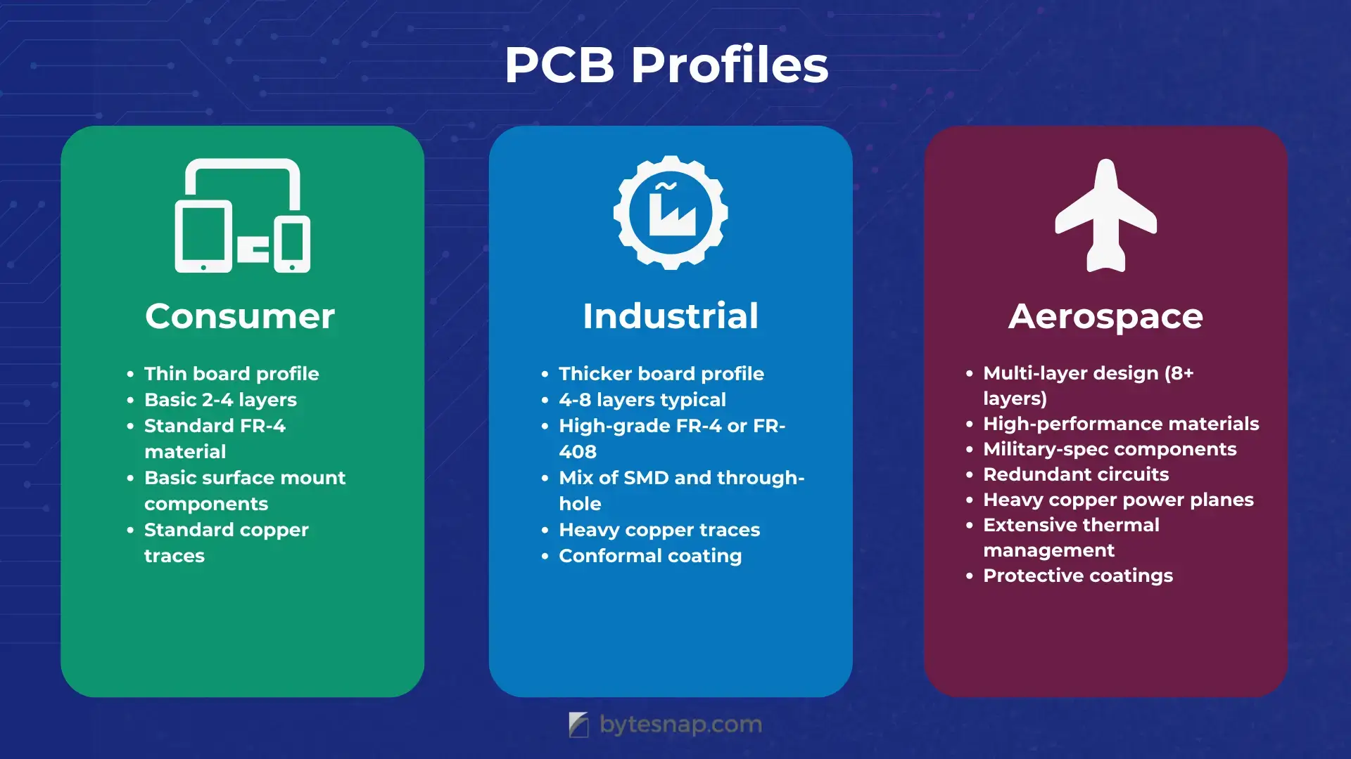
- Consumer PCBs prioritise cost-effectiveness: 2-4 layers, basic protection, high-volume manufacturing
- Industrial PCBs require robust reliability: enhanced materials, protective coatings, 10-15 year lifecycles
- Aerospace PCBs demand zero-failure performance: premium materials, extreme testing, full traceability
- 81% of UK manufacturers report difficulty finding reliable PCB design partners with sector expertise [Futureproofing Manufacturing Report, ByteSnap Design 2025]
- Design decisions made early determine 60-70% of total lifecycle costs
🎯 Key Takeaways
- Design Strategy: • Balance environmental requirements, reliability needs, and cost constraints • Consider full lifecycle implications • Follow appropriate industry standards • Implement proper design verification
- Industry-Specific Recommendations Consumer Electronics: • Focus on cost-effective designs without compromising essential functionality • Ensure compliance with relevant EMC and safety standards • Optimise for high-volume production
- Industrial Applications: • Prioritise robust design for harsh environments • Consider maintenance and serviceability • Implement appropriate redundancy measures
- Aerospace: • Focus on maximum reliability and performance • Follow strict certification requirements • Document all design decisions thoroughly
Table of Contents
PCB Design Requirements: Consumer vs Industrial & Aerospace Applications
While PCBs serve as the foundation for virtually all electronic products, their design requirements vary significantly based on their intended application, from simple consumer devices to complex, high-frequency equipment.
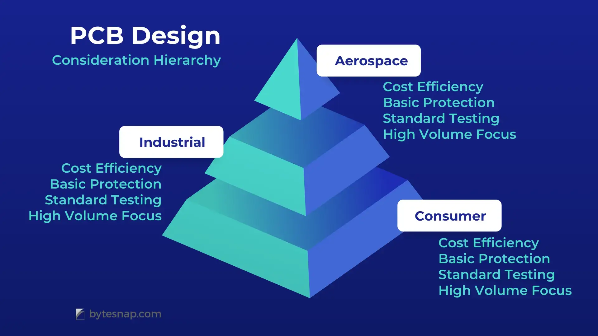
Three key aspects guide the PCB design decision-making process:
- environmental conditions
- reliability requirements
- and cost considerations
Each of these elements carries different weight depending on the sector and application.
Industrial PCB designs typically demand more robust solutions than consumer boards.
Consumer PCBs often incorporate thicker, more durable materials and protective coatings to shield against environmental factors such as dust and other contaminants.
Besides, industrial designs often include redundancy features as a safeguard against potential failures.
When we move into mission-critical environments like aerospace, the stakes are even higher.
Here, reliability and robustness are priorities. Cost implications, though important, take a secondary role. The margin for error in these applications effectively drops to zero, requiring meticulous attention to every design detail.
The Institute of Printed Circuits (IPC) has developed comprehensive standards to guide this varying spectrum of requirements.
Through IPC-A-610, they’ve established three distinct classes of electronic assemblies, ranging from general electronic products to high-performance electronic products.
This classification system directly relates to the end-use application, with Class 3 maintaining the most stringent standards and requirements.
Breakdown of IPC classes
IPCClass | Description | TypicalApplications | KeyRequirements |
|---|---|---|---|
Class 1:General Electronic Products | Limited life products; basic functionality | • Consumer electronics
• Toys
• Simple remote controls | • Basic functionality
• Cost-effective design
• Limited environmental protection
• Standard reliability |
Class 2:Dedicated Service Products | Extended life products; uninterrupted service desired | • Industrial equipment
• Network servers
• Communication systems
• Medical devices (non-critical) | • Extended service life
• Environmental protection
• Enhanced reliability
• Field serviceability |
Class 3:High Performance Products | Critical applications;continuous performance | • Aerospace systems
• Life support equipment
• Military hardware
• Critical medical devices | • Maximum reliability
• Zero failure tolerance
• Extensive testing
• Full traceability
• Environmental hardening |
How Does Operating Environment Shape PCB Design Requirements?
Your operating environment determines most of your PCB design decisions.
Industrial
Industrial applications present particular challenges because of their high-power requirements. These circuit boards drive motors and heavy machinery, demanding different design approaches than consumer electronics.
Industrial environments throw multiple challenges at your PCB simultaneously. Noise, vibration, temperature swings – each needs specific design techniques. In specialised environments, such as petrochemical facilities, ATEX approval shapes your entire design approach from the start.
Aerospace
Aerospace represents the extreme end. These boards must survive conditions that would destroy conventional PCBs:
- Extreme temperature variations
- Intense vibration and mechanical stress
- Radiation exposure
- Chemical and contaminant exposure
- Atmospheric pressure changes
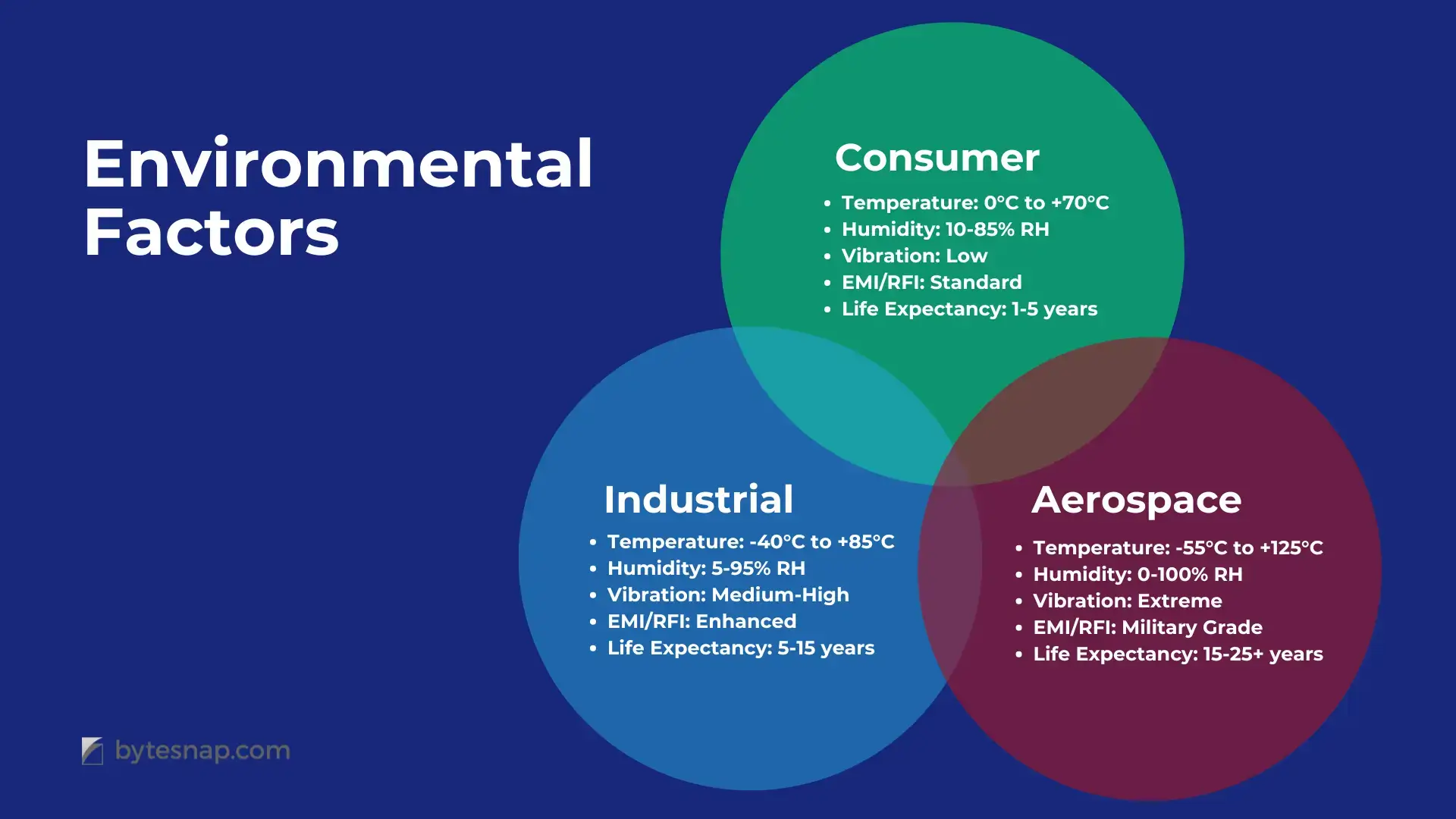
Environmental factors comparison chart
Factor | Consumer | Industrial | Aerospace |
|---|---|---|---|
OperatingTemperature | 0°C to +70°C | -40°C to +85°C | -55°C to +125°C |
HumidityResistance | 10-85% RH | 5-95% RH | 0-100% RH |
VibrationTolerance | 0.5G | 2.5G | 10G+ |
ChemicalResistance | Low | Medium | High |
AltitudeRating | Sea Level –
10,000 ft | Sea Level –
30,000 ft | Sea Level – 100,000 ft |
ExpectedLifetime | 1-5 years | 5-15 years | 15-25+ years |
Consumer
Consumer electronics face different challenges.
Whilst less extreme than aerospace, ESD and EMC requirements still matter significantly. Your PCB design determines certification success. For RF and high-speed circuits, impedance matching is important for maintaining signal integrity.
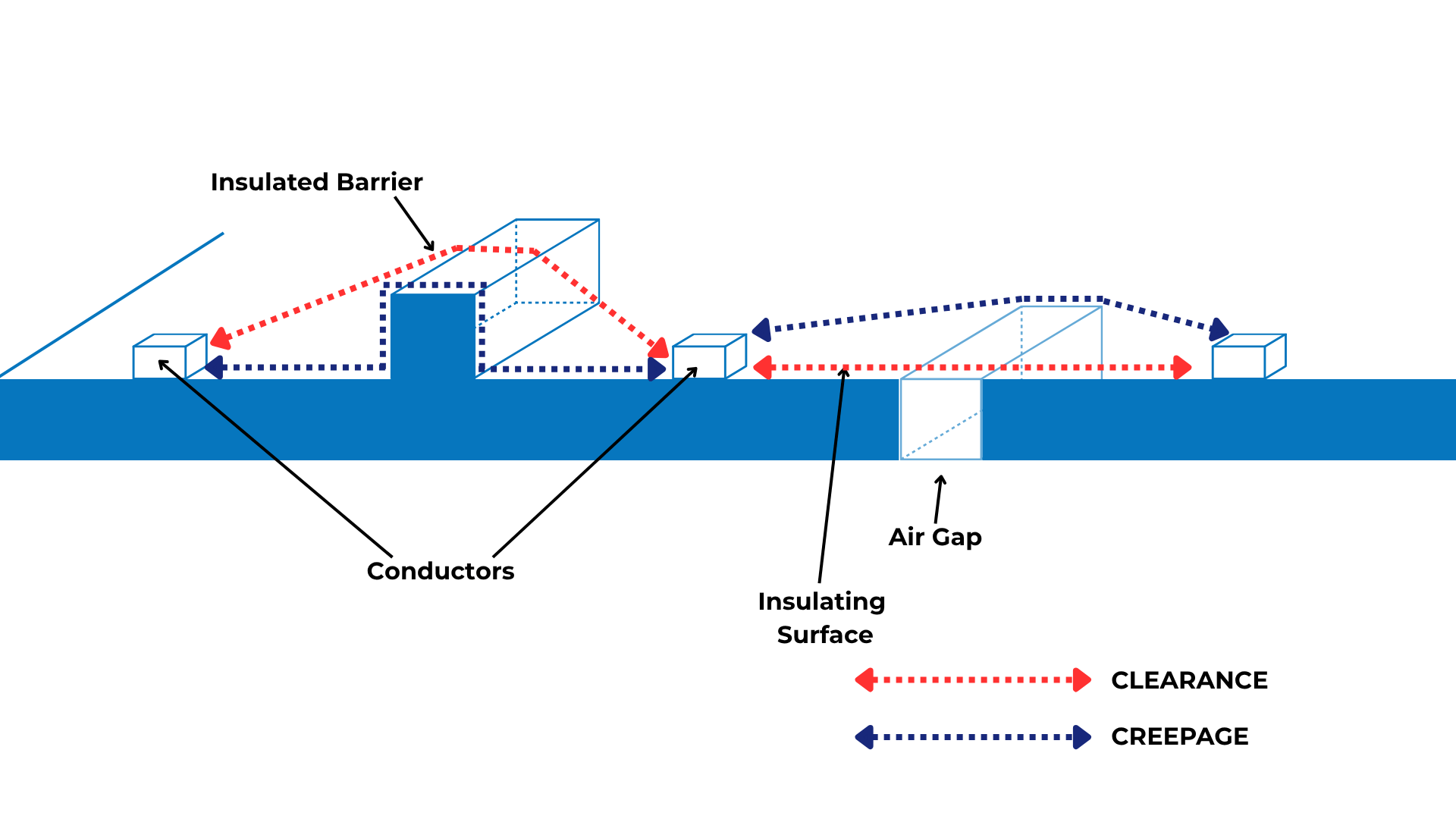
Creepage, Clearance and Pollution Degree in Industrial PCB Design
High-voltage PCBs, especially EV chargers, solar and large motor control, face unique creepage and clearance challenges.
As voltage increases, so does the risk of failure. Environmental factors like humidity, dust, altitude, pollution, and PCB material directly impact these risks.
As a result, the management of creepage and clearance is key for functional safety and regulatory compliance. PCB designers must apply voltage-based formulas or IPC/IEC tables to set minimum distances.
Standard IEC 60947-1 distinguishes four pollution degrees:
- Degree 1: No pollution or only dry, non-conductive pollution occurs.
- Degree 2: Normally, only non-conductive pollution occurs. Occasionally, however, a temporary conductivity caused by condensation may be expected.
- Degree 3: Conductive pollution occurs, or dry, non-conductive pollution occurs which becomes conductive due to condensation.
- Degree 4: The pollution generates persistent conductivity caused, for instance, by conductive dust or by rain or snow.
The higher the pollution degree, the greater the creepage and clearance distance. Mitigation of these distances is by using PCB layout techniques like slots, grooves, track width and spacing constraints. Further mitigation can be accomplished by conformal coating or encapsulation.
1.Creepage vs Clearance:
- Clearance is the shortest path through air between two conductive parts.
- Creepage is the shortest path along the surface of an insulating material.
2. Application: EV Charging Boards:
- EV chargers often operate at 230V– 380V AC, and 600 to 1200V DC under Pollution Degree 2 or 3 conditions. High voltage PCB designs must prioritise safety especially in a residential environment.
- Inadequate spacing can result in arcing, carbonisation of board material, or total failure.
- IPC-2221 and IEC 60664 standards should be followed strictly.
3. Design Strategies:
- Use wider track and gap spacing depending on expected voltage and pollution degree.
- Consider slots, notches or barriers to increase creepage on compact boards.
- Apply conformal coatings (e.g. silicone, polyurethane) to boards exposed to outdoor or high-humidity environments.
- Determine the which PCB material is best suited to your application. When selecting dielectrics and insulators for a PCB, use the comparative tracking index (CTI) to determine which material type works best for the specific application. The CTI is the maximum voltage measured in volts at which a material withstands 50 drops of contaminated water without forming conductive paths because of electrical stress, contamination, or humidity
4. Compliance and Testing:
- Refer to UL 840 and IEC 61851 (EVSE standard) for clearance/creepage requirements.
- High-voltage insulation tests and environmental simulations (humidity, dust chambers) should be part of validation.
What's the Difference Between Quality Control and Reliability Engineering?
Quality control and reliability in PCB design represent two distinct yet interconnected aspects of product development.
While quality control focuses on ensuring that a product works correctly at completion and meets all specified requirements, reliability engineering takes a longer view. It concentrates on the probability that a component will perform its intended function consistently over time, under specified operating conditions.
PCB reliability lifecycle: key elements and testing stages
Several factors influence reliability in PCB design, including initial design choices, manufacturing process control, and material selection.
These elements must work in harmony to create a board that maintains its performance throughout its intended lifespan.
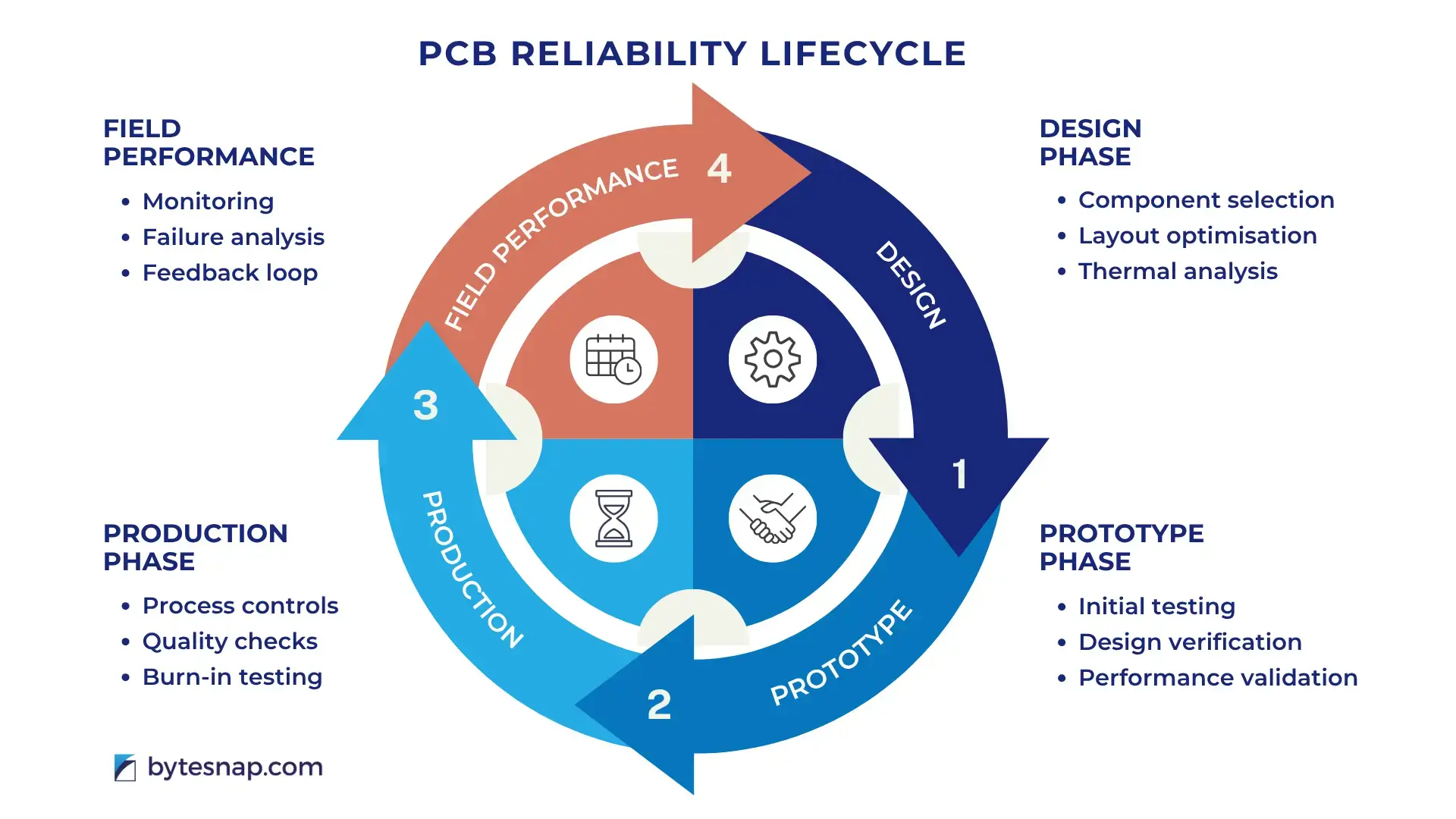
Design for reliability (DFR) takes on particular significance in industrial, medical, aeronautical and space projects.
In these applications, latent defects become unacceptable due to both the astronomical replacement costs and, more critically, the potential risk to human life.
The approach to reliability must therefore be comprehensive and systematic from the earliest design stages.
Reliability requirements and testing methods
TestType | ConsumerElectronics | IndustrialApplications | Aerospace/Defence |
|---|---|---|---|
TemperatureCycling | -0°C to +70°C, 100 cycles | -40°C to +85°C, 500 cycles | –55°C to +125°C, 1000 cycles |
VibrationTesting | Random 0.1g²/Hz | Random 0.5g²/Hz | Random 2.0g²/Hz |
HumidityExposure | 85% RH, 30 days | 95% RH, 60 days | 100% RH, 90 days |
HALT/HASS Testing | Optional | Required | Mandatory |
SaltSpray | Not Required | 500 hours | 1000 hours |
ESDTesting | 4kV HBM | 6kV HBM | 8kV HBM |
Life TestingDuration | 1000 hours | 5000 hours | 10000 hours |
CerfiticationRequired | CE/FCC | UL/CSA/CE | MIL-STD-883 |
DocumentationLevel | Basic | Medium | Full Traceability |
For instance, in aerospace applications, every component must undergo rigorous testing and validation.
The testing regime typically includes:
- Extended thermal cycling
- Vibration and shock testing
- Humidity exposure trials
- Power cycling evaluation
- Long-term stress testing
This comprehensive testing helps ensure that the PCB will maintain its performance even under the most demanding conditions.
What Drives PCB Design Costs Across Different Sectors?
The economics of PCB design involve several aspects that extend well beyond the simple material costs.
Understanding these elements helps organisations make informed decisions that balance immediate expenses against long-term value. The cost structure of printed circuit boards can be divided into two fundamental categories: hard costs and soft costs, each having an impact in the overall project economics.
Hard costs relate directly to the physical aspects of the printed circuit board itself. In industrial and aeronautical applications, these costs can be particularly significant due to the complexity of the physical board requirements. For example, copper weights and build complexity often need to be more robust in these sectors, driving up material and manufacturing expenses.
The impact on cost and sustainability becomes especially apparent when examining the complete production cycle. Soft cost drivers – those elements that might not appear on initial quotations – can significantly influence the total project investment.
These include engineering time, potential delays, and occasionally, mis-specified requirements that may drive costs upward or fail to identify essential quality and reliability needs.
Decision matrix: Cost vs Performance trade-offs
Factor | Consumer | Industrial | Aerospace |
|---|---|---|---|
OperatingTemperature | 0°C to +70°C | -40°C to +85°C | -55°C to +125°C |
HumidityResistance | 10-85% RH | 5-95% RH | 0-100% RH |
VibrationTolerance | 0.5G | 2.5G | 10G+ |
ChemicalResistance | Low | Medium | High |
AltitudeRating | Sea Level –
10,000 ft | Sea Level –
30,000 ft | Sea Level – 100,000 ft |
ExpectedLifetime | 1-5 years | 5-15 years | 15-25+ years |
Factors affecting PCB costs include:
Physical Design Elements: The size of the PCB, layer count, and overall build complexity form the foundation of cost considerations.
Via treatments and material utilisation efficiency can also significantly impact the final expense, particularly in more complex designs.
Technical Specifications: Track and gap requirements, hole specifications, and impedance considerations all influence manufacturing costs.
Also, elements such as surface finishes and copper foil weights impact both cost and performance.
The choice of materials, manufacturing processes, and quality control measures must align with the intended application while maintaining cost-effectiveness. In aerospace applications, where reliability is paramount, these decisions often lead to higher initial costs but deliver essential long-term value.
How Do You Choose the Right PCB Design Approach for Your Application?
The development of an effective PCB design requires careful consideration of multiple factors. With any PCB design project, the aim is to create layouts that not only deliver high-quality circuit boards but also ensure efficient manufacturing processes for the best return on investment. The importance of each design criterion depends on the specific requirements and compliance standards of the target industry.
Although environmental considerations, reliability requirements, and cost impact the design process, their relative importance shifts depending on the intended application. Consumer electronics may prioritise cost-effectiveness while maintaining essential functionality, industrial applications demand robust reliability in challenging environments, and aerospace applications require uncompromising performance under extreme conditions.
Successful PCB design depends on understanding these varying requirements early in the development process.
By carefully assessing and designing for specific sector needs, engineers can create solutions that effectively balance performance, reliability, and cost considerations.
Taking the Next Step
PCB Design Requirements - FAQs
Can I use the same PCB design for industrial that worked for consumer products?
Rarely works as a direct upgrade. Industrial requirements typically demand fundamental redesign: different materials (enhanced FR-4 or FR-408 vs standard FR-4), increased layer count (4-8 vs 2-4), heavier copper traces, altered component placement, enhanced thermal management, protective conformal coatings, and more extensive testing (500 vs 100 thermal cycles). The cost difference reflects these substantial technical changes, not just material upgrades.
Why do industrial PCBs cost so much more than consumer boards?
Industrial PCBs cost 1.5-2.5x more due to: thicker copper weights for high-power applications, enhanced materials rated for -40°C to +85°C operation, protective coatings against dust and contaminants, extensive testing (500+ thermal cycles vs 100), longer design time for reliability optimization, and often redundancy features. You're paying for 10-15 year service life versus 1-5 years. Based on ByteSnap Design's project data, this upfront investment typically reduces total lifecycle costs by 40-50% through fewer failures and longer deployment periods.
What happens if I specify the wrong IPC class for my PCB?
Serious consequences depending on direction. Under-specifying (using Class 1 for industrial application) risks: field failures, safety incidents, failed certification, customer liability, and expensive recalls. Over-specifying (Class 3 for consumer product) wastes budget on unnecessary testing, documentation, and materials, making your product uncompetitive. 44% of manufacturers report regulatory compliance issues when IPC class mismatches occur (ByteSnap Design survey, 2025). Get this right during specification phase, not after prototyping.
How much does aerospace PCB certification actually cost UK companies?
Certification costs for aerospace PCBs range £15,000-£100,000+ depending on: specific standards required (DO-254, MIL-STD-883), testing scope (1,000+ thermal cycles, vibration, radiation), documentation level (full traceability required), and recertification frequency. However, certification represents only 15-20% of total aerospace PCB costs. The bigger expenses come from: premium materials, extensive design validation, specialized manufacturing processes, and comprehensive testing. Budget 4.0-6.5x consumer PCB baseline costs for complete aerospace-grade development.
What's the biggest mistake companies make when specifying PCB requirements?
Underestimating soft costs and lifecycle implications. Companies focus on initial PCB manufacturing cost (30-40% of total impact) and ignore: engineering redesign time when specifications wrong, testing and validation expenses, recertification costs, production downtime during component obsolescence, and opportunity cost of diverted engineering resources. Second biggest mistake: not involving PCB design expertise during architecture phase when 60-70% of lifecycle costs get locked in.
How do I know if my PCB design partner understands my sector requirements?
Ask these specific questions:
(1) Show me three similar projects in [your sector] with actual operating temperature data and failure rates?
(2) What IPC class do you recommend and why - explain the trade-offs?
(3) How do you handle component obsolescence in designs with 10+ year lifecycles?
(4) What's your experience with [your specific certification, e.g. ATEX, DO-254, etc.]?
Red flags = generic answers, no sector-specific examples, pushback on certification questions, or focus only on cost.
81% of UK manufacturers report finding partners with right expertise as their top challenge (Futureproofing Manufacturing Industry Report, ByteSnap Design, 2025).

With over 30 years of experience in electronics design and manufacturing, Conrad brings a wealth of knowledge to the ByteSnap team. His extensive career has spanned diverse industries, including the petrochemical, industrial, security, and commercial sectors.
Previously, Conrad’s entrepreneurial spirit led him to establish and manage his own PCB population factory in South Africa. This hands-on experience deepened his understanding of the intricacies of electronics manufacturing.
Conrad’s decision to join ByteSnap was driven by his desire for continuous growth and the opportunity to work with a UK-leading electronics design house. He says, “Working at ByteSnap is interesting, challenging, and completely enjoyable.”
Away from circuits and components, Conrad enjoys exploring new places, museums, and football.