⏩ TL;DR: How much power is actually "safe" in Zone 0?
- Designing for Zone 0 (Ex ia) is a game of tight margins. For Gas Group IIC, you are usually fighting to stay under 29V and 1.3W, but those aren't the numbers that will kill your design. The real challenge is stored energy.
- If your circuit stores more than 40 microjoules, it has the potential to cause a spark that ignites the atmosphere. In 2026, where CTOs want high-performance sensors and wireless comms on the edge, "simple" passive limiting often isn't enough. You have to balance the T-rating (thermal) against the electrical energy, often using active current-limiting to keep your footprints small and your performance high.
Table of Contents
Why "keeping power low" isn't enough for Zone 0
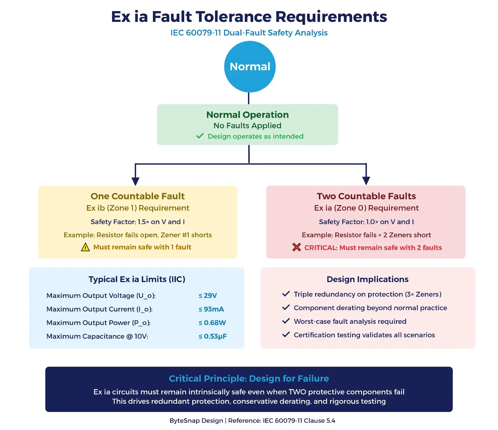
In Ex ia design, low power consumption is only one part of the equation. You’re managing the physical ability of your circuit to ignite an atmosphere even after two simultaneous countable faults occur.
For Zone 0 environments, where explosive gases are present continuously, a single failure could be catastrophic. You must define a mathematical energy envelope that remains safe under the most onerous conditions. This involves looking at “non-countable” faults, like PCB track clearances or component ratings, which the Notified Body will evaluate as part of the worst-case scenario.
If you haven’t accounted for these energy discharge paths during the initial schematic design, you risk a total hardware redesign once the certification process begins.
Can your circuit survive two simultaneous failures?
For Ex ia (Zone 0) certification, your design must remain intrinsically safe even when two protective components, such as Zener diodes or current-limiting resistors, fail short or open.
This “Dual-Fault” requirement dictates the safety factors you must apply:
- Normal Operation + One Fault: You must maintain a 1.5x safety factor on both voltage and current.
- Normal Operation + Two Faults: You must maintain a 1.0x safety factor.
In practice, this leads to triple redundancy. If your protection circuit relies on Zener diodes to clamp a voltage rail, you will typically use three diodes in parallel. If two fail, the third must still be capable of shunting the full fault energy safely.
This “Design for Failure” mindset requires conservative component derating that goes far beyond standard commercial electronics practice.
Hardware trade-offs – High performance vs. IS limits
Modern electronics expectations – embedded processors drawing 500mW, Bluetooth 5.0 modules consuming 300mW peaks, multi-channel sensor arrays – directly conflict with the severe constraints of Ex ia power budgets.
When we designed the WAND Remote Data Collector for Inductosense, we had to deliver an 8-channel ultrasonic IoT device with 5+ year battery life whilst meeting Zone 0 certification for Gas Group IIC T4. We couldn’t just specify standard components and hope the power budget worked out.
We built the entire system around ultra-low power operation from day one. The final device consumes under 800mW under heavy load. It still manages 200-metre Bluetooth 5.0 range and processes signals from eight ultrasonic thickness sensors monitoring pipeline corrosion on offshore platforms.
There’s no single component that fixes this problem. You need system-level power management where every subsystem shuts down completely between measurements. Partial sleep modes don’t cut it.
What happens when the Notified Body breaks your design?
Most engineering teams design for operational reality. The notified body tests for the worst-case fault condition. That gap is where expensive PCB respins happen.
You must account for:
- Minimum resistance paths (not the values on your schematic)
- Maximum line voltage from your power supply or associated apparatus
- Component failures that short-circuit current-limiting resistors
- Zener diode failures that remove voltage clamping
The notified body will deliberately break your circuit in the worst possible ways. If you haven't already designed for those exact failure modes, you'll be redesigning the PCB when they find the weak point.
We've seen boards fail certification because a junior engineer added a 10µF decoupling capacitor late in the layout process without checking the total capacitance budget. It's an easy mistake to make. The lab bill for retesting isn't cheap.
Why three Zener diodes are better than two
Ex ia circuits need redundancy in protective components. Voltage-limiting Zener diodes typically use three diodes in the protection circuit. Any two can fail and the third still maintains safe voltage limits.
Current-limiting resistors work the same way. Multiple series resistors with defined power ratings mean that if one fails open, you still have sufficient resistance in the circuit.
You might look at this and think it’s over-engineering. It’s not. It’s the minimum requirement for proving your circuit stays intrinsically safe under two-fault conditions.
Fault Scenario Analysis Matrix
IEC 60079-11 Dual-Fault Safety Analysis Requirements
| Scenario | Fault Count | Safety Factor | Voltage Limit | Current Limit | Energy Limit | Certification Level |
|---|---|---|---|---|---|---|
| Normal Operation | 0 | 1.0× | U₀ | I₀ | C₀/L₀ per tables | Operational parameters |
| Single Countable Fault | 1 | 1.5× | 1.5 × U₀ | 1.5 × I₀ | Consider worst-case | Ex ia/ib requirement |
| Two Countable Faults | 2 | 1.0× | U₀ | I₀ | Critical failure mode | Ex ia only |
Fault Examples to Analyse
- Component short circuits: Zener diode fails short, limiting resistor fails open
- PCB track failures: Copper track opens under thermal stress, creating unintended current path
- Connection failures: Terminal wire breaks, connector pin intermittent
- Supply overvoltage: Input power exceeds rated maximum due to power supply fault
- Multiple simultaneous: Worst combination of above that creates highest energy discharge
Design Response
Designing layouts that survive the spark ignition test
IEC 60079-11 specifies minimum creepage and clearance distances based on voltage and pollution degree. For 24V circuits in pollution degree 2 environments, minimum creepage typically exceeds 3mm.
This affects:
- Track spacing between intrinsically safe and non-intrinsically safe sections (requires physical barriers or >50mm separation)
- Component placement ensuring high-voltage parts don’t compromise IS circuits through surface tracking
- Conformal coating selection where coating reduces required spacing but must be certified as reliable over product lifetime
Our PCB layouts for ATEX products always undergo design rule checking specific to IEC 60079-11 requirements before fabrication. This catches spacing violations before the board goes to manufacture. It’s cheaper than discovering the problem when the notified body puts your board under a microscope and fails it for a 2.8 mm gap that should have been 3 mm.
Zener Barriers vs. Galvanic Isolators: Which is right for your site?
Choosing between shunt diode barriers and galvanic isolators affects component costs, installation complexity, and, ultimately, your overall industrial hardware development strategy.
(As well as how much grief your client’s maintenance team will give you in five years…)
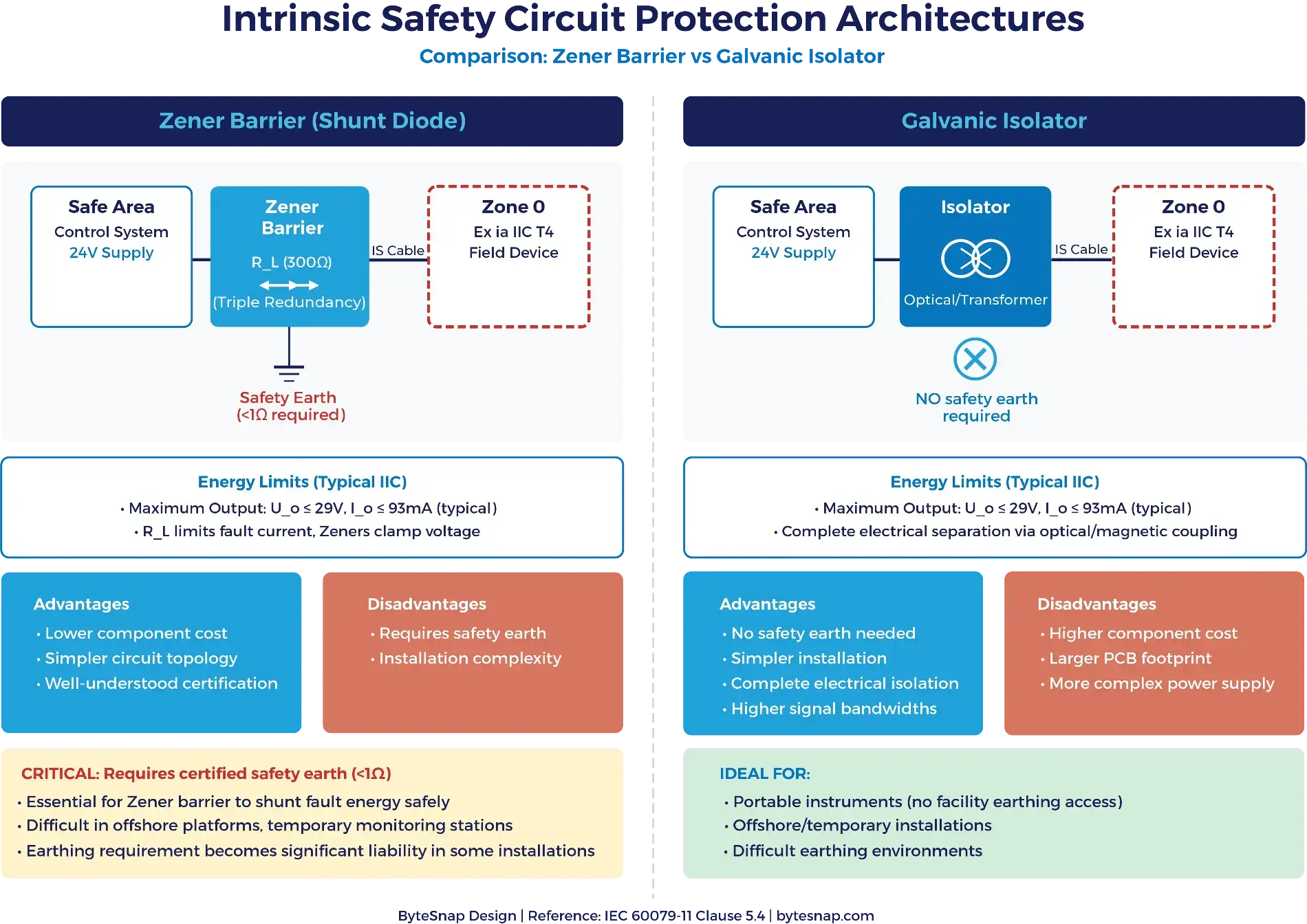
Lowering component costs with Shunt Diode (Zener) Barriers
Advantages:
- Lower component costs (£50–200 per channel for standard barriers)
- Simple circuit topology
- Certification bodies understand them
Critical disadvantage:
You need a certified, ultra-low resistance safety earth connection (typically <1Ω).
The Zener barrier relies on this earth to shunt fault energy safely. If you’re installing on an offshore platform, a temporary monitoring station, or an older industrial facility where reliable earthing is difficult, this requirement becomes a problem.
Engineering details:
The series limiting resistor (R_L) sets the maximum fault current. For a 28V barrier with 93mA maximum current into a Zone 0 IIC circuit, R_L usually runs above 300Ω.
You’ll use three Zener diodes in series to clamp voltage, each rated for the full fault energy dissipation.
The barrier sits between the hazardous area circuit and the safe area control system, with the Zener cathodes connected to safety earth.
Eliminating the safety earth requirement with isolation
Advantages:
- No safety earth needed
- Complete electrical separation between safe and hazardous areas
- Simpler installation in difficult earthing environments
- Higher signal bandwidths (optical or transformer coupling)
Disadvantages:
- Higher component costs (£200–600 per channel)
- Larger PCB footprint
- More complex power supply design (you need isolated power rails)
When does the extra cost make sense?
For the WAND-RDC project, the device operates remotely in hazardous zones with no access to facility earthing. Galvanic isolation was the only option. Same story for the portable intrinsically safe device we developed for Geotechnical Instruments. Field environments don’t come with reliable earth connections.
On large sites where cable runs stretch for kilometres, the cost of running dedicated safety earths can actually exceed the component cost difference. We’ve had clients switch to isolation purely on the grounds of installation costs.
Choosing parts that won't kill your energy budget: why your capacitors are the biggest threat to compliance
The stored energy equations (E = ½CV² for capacitors, E = ½LI² for inductors) control every component you select. For Gas Group IIC with 40 microjoules minimum ignition energy, you run out of energy budget fast.
Here’s a typical scenario: you need 10V supply voltage for your MCU and sensor interface. IEC 60079-11 Table A.2 limits your total capacitance to roughly 3 microfarads for IIC at this voltage.
That’s everything:
- Power supply bulk capacitance
- MCU supply decoupling
- Sensor interface filtering
- PCB parasitic capacitance
- Cable capacitance (about 95nF per kilometre for standard instrumentation cable)
How do we handle this?
Instead of one massive bulk capacitor, we often have to split the capacitance across multiple protected nodes or use series resistors to limit the discharge current.
It’s a tedious balancing act: you need enough “C” to keep the MCU stable during a WiFi burst, but little enough to satisfy the spark ignition test. If you get this wrong, you’ll find yourself adding expensive, board-space-hogging encapsulated components just to pass.
When we designed the WAND-RDC, this constraint directly influenced our power architecture. We couldn’t just drop in large bulk capacitors for energy storage. We had to rethink the entire power architecture:
- Multiple smaller capacitors in parallel rather than single large values
2. Multiple smaller capacitors in parallel rather than single large values
3. Ultra-low quiescent current regulators to minimise required supply filtering
4. Dynamic power management where subsystems power down completely between measurements
⚡ Benchmark your design's energy limits
Why you can't just use any rechargeable cell in Zone 0
Rechargeable batteries are generally banned in Ex ia circuits because of thermal runaway risk. For the WAND-RDC’s 5+ year operational life, we specified:
- Non-rechargeable lithium thionyl chloride cells (certified to UN38.3)
- Series current-limiting resistors preventing short-circuit currents exceeding safe limits
- Protective enclosure design ensuring cell containment even under mechanical stress
- Temperature monitoring via the device firmware to prevent operation outside safe temperature ranges
The battery selection alone required coordination with Custom Power for Ex-certified battery packs meeting both ATEX Zone 0 and UN transport regulations.
Capacitors: Energy Reduction Strategies
When bulk capacitance exceeds the limits in IEC 60079-11 Table A.2, you need strategies to reduce stored energy without losing circuit stability. Here are three approaches that work:
1. Series capacitor banks: Two 2µF capacitors in series provide 1µF effective capacitance but limit energy if one fails short-circuit. You’re adding redundancy whilst reducing the total stored energy.
2. Lower voltage rails: Reducing voltage from 12V to 3.3V increases permissible capacitance by a factor of >10 (energy scales with V²). If you can run your circuit at a lower voltage, the capacitance budget opens up significantly.
3. Active discharge circuits: Fuse-protected discharge resistors that activate when voltage exceeds safe limits. These add complexity but give you headroom when passive limiting won’t cut it.
The choice between these depends on your circuit topology and whether you can tolerate the board space for series banks or the quiescent current for active discharge circuits. There’s no universal answer.
Case Study: Delivering an 8-channel IoT sensor in Zone 0
The Inductosense WAND Remote Data Collector demonstrates what happens when you build intrinsic safety into the architecture from day one rather than retrofitting it at the end.
Technical Specifications:
- Certification: ATEX Zone 0, II 1 G Ex ia IIC T4 Ga (-40°C < Ta < +130°C)
- Power budget: <800mW average under operational load
- Battery life: 5+ years from non-rechargeable lithium cells
- Communication: Bluetooth 5.0 Long Range, 200-metre range
- Channel capacity: 8 ultrasonic sensors simultaneously monitored
- Operating environment: Offshore oil and gas platforms, chemical plants, refineries
Power Budget Breakdown:
From our earliest design discussions with Inductosense, the power budget controlled every architecture decision:
1. Microcontroller selection: Ultra-low-power ARM Cortex-M processor with deep sleep modes drawing <5µA. Standard MCUs pull 50-100µA in sleep. That difference matters when you’re targeting 5+ year battery life.
2. Wireless interface: Bluetooth 5.0 module optimised for long-range, low-power operation with connection event spacing maximised. We scheduled wireless transmissions in batches rather than transmitting every sensor reading immediately.
3. Ultrasonic driver: Custom ASIC design providing precisely controlled pulses within energy limits. Off-the-shelf ultrasonic drivers consume too much power and don’t give you the control needed for Ex ia compliance.
4. Firmware optimisation: Sophisticated power state machine ensuring subsystems only activate when required. The GPS receiver, for example, only powers up during location acquisition, then enters ultra-low-power standby.
The result? A device that collects wall thickness data from eight pipeline locations, processes the ultrasonic signals, stores 1500 readings, and transmits data wirelessly, all whilst meeting the stringent energy limits for Zone 0 IIC certification.
How we achieved a 5-year battery life under Ex ia limits:
We used several advanced power management techniques in developing the world-first 8-channel ATEX Zone 0 IoT sensor:
- Time-division multiplexing of the eight ultrasonic channels, ensuring only one channel energises at any instant
- Adaptive sampling rates based on corrosion progression rates, reducing power when slower sampling suffices
- Wireless communication batching, where multiple sensor readings accumulate before Bluetooth transmission
- Temperature-compensated algorithms accounting for how thermal effects influence both measurement accuracy and power consumption

Modernising field gas analysis within IIC constraints
Before the WAND-RDC, we demonstrated similar power budgeting expertise with the Geotech 5000 series of landfill and biogas analysers – the industry’s first commercially available gas analysers approved for Zone 0 environments, incorporating smartphone-like features.
Project Specifications:
- Certification: Zone 0 (gas group IIC)
- Power budget: <800mW under heavy operational load
- Platform: Windows CE operating system—a first for Zone 0 gas analysis equipment
- Features: GPS tracking, Bluetooth connectivity, accelerometer, digital compass, colour touchscreen interface
Power Budget Challenge:
Geotech needed to replace ageing gas analysis equipment with modern technology offering:
- Sub-10-second gas measurement cycles
- GPS location tracking for field survey mapping
- Bluetooth data transfer to eliminate manual logging
- Full-colour touchscreen for intuitive operation
- Multi-sensor capability for CH₄, CO₂, O₂, H₂S and balance gas
Each of these features demanded power. The GPS receiver alone typically consumes 50-80mW continuous. The colour LCD backlight required 150-200mW. The Windows CE platform needed sufficient processing headroom for responsive UI performance.
Our Solution:
Using a full custom board design and writing all device software in-house, ByteSnap implemented:
- Adaptive GPS management: GPS powered only during location acquisition, then entering ultra-low-power standby
- Backlight dimming algorithms: Automatic adjustment based on ambient light sensor, reducing power by 60% in bright conditions
- Sensor duty cycling: Gas sensors powered in sequence rather than simultaneously, reducing peak current draw
- Processor sleep states: Windows CE configured for aggressive power management, entering deep sleep between user interactions
The result consumed fewer than 800 mW even when running measurement cycles with full UI interaction, well within Zone 0 IIC energy limits, while delivering functionality that transformed the field gas analysis workflow.
How to pass the Notified Body assessment on the first try
Design flaws discovered late in the ATEX/IECEx certification process create multiple problems:
Time costs: ATEX certification typically requires 8-12 weeks for well-designed products. Discovering energy budget violations, inadequate component derating, or PCB layout issues during notified body assessment extends timelines by 3-6 months whilst designs are corrected and retested.
Financial costs: A single board respin for a four-layer PCB runs £3,000-5,000 including assembly. Retesting at the notified body adds £5,000-8,000 per iteration. Component changes requiring new supplier approvals or re-sourcing certified parts multiply costs further.
Opportunity costs: Delayed market entry in sectors like oil and gas or chemical processing, where capital projects operate on strict schedules, means missed contracts and revenue. One client came to us after their first certification attempt failed. The six-month delay cost them a £2M installation contract that went to a competitor with certified equipment ready.
Specialist engineers at our electronics design consultancy can help you avoid these pitfalls by integrating compliance into your project from day one.
Our process for eliminating late-stage redesign loops
Our ATEX design process integrates intrinsically safe power budgeting from initial concept:
- Feasibility assessment: Before committing to detailed design, we model the energy budget against functional requirements, identifying conflicts early
- Component pre-certification: Our database tracks dual-certified components (both ATEX and IECEx) from approved suppliers, avoiding sourcing issues during certification
- Design rule verification: PCB layouts undergo automated checking against IEC 60079-11 creepage, clearance, and energy requirements
- Pre-compliance testing: In-house verification of voltage/current limits, energy storage, and thermal performance before formal notified body submission
This process enabled the WAND-RDC to achieve certification within the planned timeline despite its technical complexity, delivering 1,000 units into production on schedule.
Does your next hazardous area product need a review?
FAQs
Q: What are the maximum voltage, current and power limits for a Zone 0 (Ex ia) intrinsically safe circuit?
There are no universal "hard numbers" for intrinsically safe limits. Instead, IEC 60079-11 defines complex ignition curves based on gas group classification. For the most restrictive gas group (IIC), circuits typically operate below 29V, with many designs targeting under 1.3W continuous power for simpler circuits. However, the actual safe limits depend on the specific gas or vapour group present and the circuit's stored energy in capacitance (C) and inductance (L).
Q: How do capacitance and inductance (C and L) impact the overall energy budget of an IS design?
Stored energy is the primary ignition concern, not continuous power. The energy stored in capacitors (E = ½CV²) and inductors (E = ½LI²) can discharge as a spark during circuit faults. For gas group IIC, the minimum ignition energy is approximately 40 microjoules. This means that at 10V, the maximum permissible capacitance is only 3 microfarads according to IEC 60079-11 Table A.2—a severe constraint for modern electronics.
Q: How does the total power budget of a device relate to its temperature class (T-rating)?
The T-rating (T1 through T6) indicates maximum surface temperature under fault conditions. Even when electrical energy remains intrinsically safe, power dissipation generates heat. A T4 rating (135°C maximum surface temperature) is common for industrial applications, but achieving this whilst maintaining functionality often requires sophisticated thermal management and power optimisation throughout the design.

Dunstan is a chartered electronics engineer who has been providing embedded systems design, production and consultancy to businesses around the world for over 30 years.
Dunstan graduated from Cambridge University with a degree in electronics engineering in 1992. After working in the industry for several years, he co-founded multi-award-winning electronics engineering consultancy ByteSnap Design in 2008. He then went on to launch international EV charging design consultancy Versinetic during the 2020 global lockdown.
An experienced conference speaker domestically and internationally, Dunstan covers several areas of electronics product development, including IoT, integrated software design and complex project management.
In his spare time, Dunstan enjoys hiking and astronomy.
ByteSnap Resources:
Intrinsically Safe Energy Storage Calculator: Instantly model your design’s safety factors.
ATEX & Intrinsically Safe Design:
- ATEX Product Design Services
- ATEX Design Guide: Tips for Successful Development
- ATEX and Intrinsic Safety: Design for Harsh Environments
Case Studies:
- Award-Winning Zone 0 Case Study: How we achieved Ex ia certification for an 8-channel IoT sensor.
- Intrinsically Safe Win CE Device for Geotech
- WAND Remote Data Collector – IoT Product of the Year 2022
Low Power Design (relevant to IS budgets):
Standards & Regulatory Resources (External Links)
IEC Standards:
- IEC 60079-0: Explosive Atmospheres – General Requirements
- IEC 60079-11: Intrinsic Safety “i” Protection
- IEC 60079-14: Electrical Installations Design, Selection and Erection
- IEC 60079-25: Intrinsically Safe Electrical Systems
UK/EU Regulations:
- UK ATEX Equipment Directive (Statutory Instruments)
- EU ATEX Directive 2014/34/EU
- HSE Guidance on DSEAR (Dangerous Substances and Explosive Atmospheres Regulations)
IECEx Scheme:
Spark Ignition & Energy Calculations:
- Spark Ignition Assessments in Intrinsically Safe Circuits (LinkedIn) – Detailed worked examples
- 10 Mb/s SPE Powering in Intrinsically Safe Systems (IEEE) – Energy limit calculations
Gas Group Classifications:
Component Selection:
- Inductosense WAND Sensors ATEX Certification – Real-world Zone 0 sensor specifications
Industry Best Practices:
Notified Bodies & Testing Laboratories
UK:
- Sira Certification Service – Major UK notified body
- CSA Group – ATEX/IECEx certification
Europe:
- DEKRA Testing and Certification – Global certification services
- TÜV SÜD – German notified body
International:
- FM Approvals – North American certification
- UL Solutions – Global safety science company