
⏩ TL;DR
Shrinking a board is a thermal and EMC decision before it's a layout one. Cutting board area removes the copper that would otherwise be used for heat spreading and clean return paths, so every square millimetre you save has to be recovered somewhere else, through heavier internal copper, or a tighter HDI and reference-plane strategy. Sequence thermal and EMC planning after layout and you'll end up reworking a finished board instead of adjusting a placement
Table of Contents
What actually changes when you shrink a board?
Most miniaturisation guides treat it as a parts-selection exercise: pick smaller passives, place them closer, run the autorouter, etc.; but real projects don’t tend to work like that.
Compressing a board removes the open copper area normally relied on for convection and heat spreading, which pulls high-speed traces and sensitive analogue circuitry closer together than before. So, coupling that used to be negligible starts showing up on the bench, and it usually forces a move from standard through-hole vias to laser-drilled microvias. That’s because there’s not enough room to route escape channels through a plated through-hole on every layer.
We’ve found it works well to plan the thermal and EMC strategy before placing parts as it makes these effects manageable.
Leave them until after routing and you’re debugging a board that already exists.
Fitting a security camera into a tennis ball
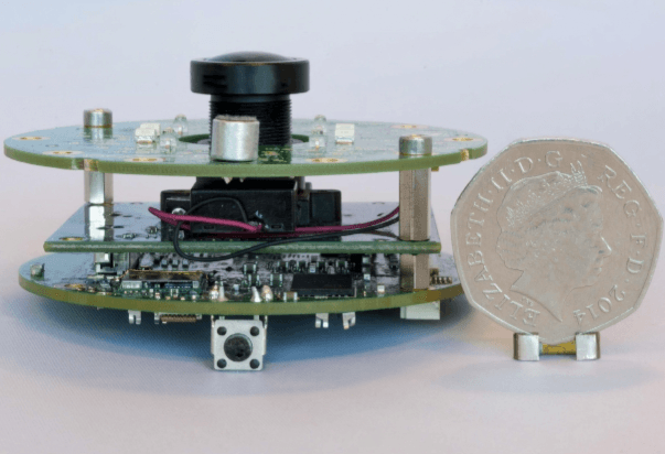
Here’s an example of this trade-off from one of our previous projects. ByteSnap Design and Cocoon won the 2016 Design Team of the Year at the British Engineering Excellence Awards for the Cocoon smart home security system.
This was a device roughly the size of a tennis ball that had to fit an HD camera with night vision, Wi-Fi, Bluetooth 4 LE, an eight-LED infrared array, a 6.5W speaker amp and a 1GHz processor into a spherical plastic enclosure with no fan and no external heatsink.
The board itself came in at 68mm in diameter. Getting there meant planning for heat and EMC before layout started, catching problems on paper rather than at the compliance chamber.
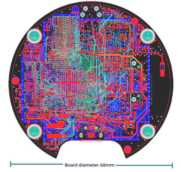
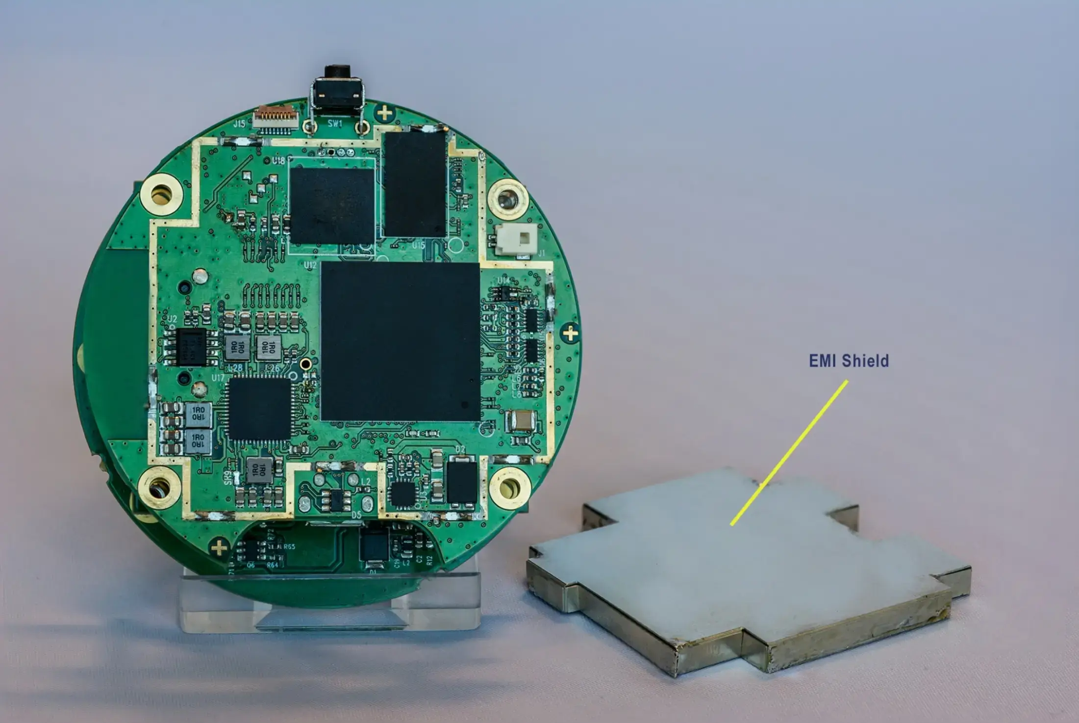
The sensitive analogue microphone circuitry, essential for the device’s infrasonic detection, had to sit away from the high-performance digital section built around the processor, or the audio noise floor would have made the product unusable. ByteSnap Design’s built in EMI shielding as a contingency for the RF and digital sections before formal compliance testing began, and the board passed CE, FCC and R&TTE testing without needing it.
Cocoon’s own COO, Dan Conlon, put it plainly afterwards: ByteSnap’s expertise helped bring the product to market in a short time frame, and Cocoon had no doubts about working with the team again. That’s what miniaturisation projects actually need from a design partner, someone who’s planned for the thermal and EMC consequences of density before the board is fabricated.

Managing heat without airflow
Standard boards lean on open air and convection. Sealed, compact enclosures, the kind you’ll find on IP-rated industrial housings as much as on consumer devices like Cocoon, trap that heat instead. Put a processor next to a power management IC in that kind of enclosure and a local hotspot builds fast.
The fix has to come from the board itself:
- Thermal via arrays: Plated vias under the exposed ground pads of QFNs and BGAs pull heat away from the component and into inner copper layers, where it can spread out rather than pool.
- Heavier inner copper: Specifying 2oz copper on internal layers turns the substrate itself into a lateral heat spreader, reducing peak temperature at the hot component without adding a single extra part.
- Deliberate component placement: Keeping temperature-sensitive parts, crystal oscillators and precision analogue circuits especially, out of the thermal wake of switching regulators and high-current traces.
- Thermal interface material to the case: Where the enclosure allows it, a thermal pad between a hot component and the housing wall gives heat somewhere to go beyond the board itself.
How much difference the enclosure material makes is worth knowing before you commit to a design.
An aluminium enclosure with proper ventilation can run 20 to 40°C cooler than an equivalent sealed plastic housing (PCBSync, 2026), a large swing for a component sitting close to its rated maximum. If your product needs a sealed plastic case for cost or IP-rating reasons, and many do, that gap has to be closed on the board, through copper, vias and placement, because the enclosure isn’t going to close it for you.
How much microvia density can you get?
Once you’re routing 0.4mm or 0.5mm pitch BGAs, standard through-hole vias stop being practical. Every through-hole via blocks routing space on every layer it passes through, whether you need the connection on that layer or not.
High-density interconnect (HDI) design solves this with laser-drilled microvias that span a single dielectric layer instead of the whole stack. IPC-2226, the sectional design standard covering HDI printed boards, sets the working limit at a depth-to-diameter aspect ratio of 1:1 or below, and most fabricators recommend staying closer to 0.75:1 in practice for consistent copper plating during fabrication (AllPCB, 2025).
Push past that and you risk voiding in the plated barrel, which shows up as an intermittent connection during thermal cycling rather than a clean failure on the test bench.
You’ll also choose between staggered and stacked microvias. Staggered vias, offset from layer to layer, cost less and yield better. Stacked vias sit directly on top of each other through multiple layers, which saves more routing area but needs copper fill and planarisation, adding real cost to the panel.
The dielectric thickness you choose for a stackup has a second, less obvious benefit. Signal-spacing guidelines for controlling crosstalk are often expressed as a multiple of H, the distance between a signal trace and its nearest reference plane.
A thinner dielectric therefore reduces the trace spacing needed to maintain the same H-based spacing ratio. It also brings the reference plane closer to the trace, helping to confine the signal fields more tightly and allowing denser routing without necessarily increasing crosstalk.
Does shrinking a board tighten EMC margins?
Usually, yes, and it’s the part of miniaturisation that catches engineers out most often.
Shrinking board area tempts you to cut into ground planes to make room for signal routing. Interrupting a return path underneath a high-speed trace creates a common-mode noise source and, in the worst case, an unintentional slot antenna, which is a reliable way to fail an emissions test that a larger board would have passed comfortably.
Two things help protect against this as density goes up. Keep return paths unbroken underneath every high-speed signal, even when it costs you routing convenience elsewhere. And treat the RF and digital sections as separate physical zones from the start, the way the Cocoon board separated its sensitive microphone circuitry from the processor, rather than trying to shield your way out of a layout decision after the fact.
0201s, BGAs and assembly yield
A miniaturised board that routes cleanly in CAD still needs to assemble cleanly on a production line, and that’s a separate problem. As passive components shrink to 0201 footprints, yield drops quickly if the pad design isn’t balanced.
The classic failure mode is tombstoning. If one pad of a small passive connects to a wide copper pour and the other connects to a narrow trace, the solder on the narrow pad reflows first. Surface tension then pulls the component upright on the cooler end, and it never makes contact on the other. Solder-mask-defined pads and thermal relief spokes on ground connections, backed by stencil apertures matched to the pad geometry, help keep that risk down at volume.
Fine-pitch BGAs bring a related problem: placement accuracy. At 0.4mm pitch, the margin for misalignment during pick-and-place is small, and X-ray inspection becomes the only reliable way to confirm a joint underneath the package rather than assume it from a visual check.
So how much does a smaller board cost?
This is where the commercial case gets made or lost. HDI fabrication typically costs 20 to 60% more per panel than an equivalent-layer-count standard multilayer board, driven mainly by laser drilling and the extra lamination cycles a sequential HDI build-up needs (WellPCB, 2026). It’s best to factor in that cost early on in a project, rather than discovering it after a design is locked.
Whether that premium is worth paying comes down to what it buys you elsewhere. A smaller board usually means a smaller enclosure, less material, lower tooling cost and reduced shipping volume, all of which offset part of the fabrication premium at scale.
It can also mean fewer layers overall, since HDI microvias sometimes let you route the same density in six to eight layers that would otherwise need ten to twelve. Whether the trade-off pays for itself depends heavily on volume and enclosure cost, so it’s a good idea to run that calculation before the stackup is committed.
Key takeaway
Board miniaturisation is a set of trade-offs across thermal design, HDI routing, EMC margin and fabrication cost that all move together. Treating them as one connected problem from the start of a project gets a board that works the first time, solving them as separate issues in sequence usually means reworking a finished design.
Get your board reviewed before it's fabricated
PCB Miniaturisation FAQs
What is HDI in PCB design?
High-density interconnect (HDI) is a PCB construction method using laser-drilled microvias, finer traces, tighter layer spacing and higher connection density than standard multilayer boards. It lets designers route fine-pitch BGAs and dense component placement that standard through-hole vias can’t support, often in fewer total layers than an equivalent standard board would need.
What is the maximum microvia aspect ratio for reliable plating?
IPC-2226 sets the working ceiling at 1:1, depth to diameter, but most fabricators recommend staying at or below 0.75:1 in practice. Pushing past that increases the risk of voiding in the plated copper barrel, which tends to surface as an intermittent connection during thermal cycling rather than a clean failure at test, making it harder to catch before it reaches the field.
Does miniaturisation always increase overall product cost?
Not necessarily. HDI fabrication itself typically costs 20 to 60% more per panel than standard multilayer, but a smaller board often reduces enclosure size, material cost, tooling and shipping volume. Whether the trade-off pays for itself depends on production volume and how much of that saving offsets the fabrication premium, so it’s worth modelling before the stackup is locked.
When should thermal simulation happen in the design cycle?
Run thermal simulation during component placement, before routing starts. Moving a high-dissipation IC or adding a thermal via array is straightforward on paper. Reworking a fully routed HDI board because a regulator throttles during bench testing costs real schedule time and wastes a prototype run that an earlier simulation pass would have avoided.
What is the 3H rule in PCB design?
The 3H rule is a spacing guideline for controlling crosstalk and edge radiation: the gap between a signal trace and an adjacent copper feature should be at least three times the dielectric thickness between the signal layer and its nearest reference plane (Cadence Design Systems, 2023). Because HDI stackups use thinner dielectric layers, the same 3H multiple needs less physical space, part of why HDI supports tighter routing.

Dunstan is a chartered electronics engineer who has been providing embedded systems design, production and consultancy to businesses around the world for over 30 years.
Dunstan graduated from Cambridge University with a degree in electronics engineering in 1992. After working in the industry for several years, he co-founded multi-award-winning electronics engineering consultancy ByteSnap Design in 2008. He then went on to launch international EV charging design consultancy Versinetic during the 2020 global lockdown.
An experienced conference speaker domestically and internationally, Dunstan covers several areas of electronics product development, including IoT, integrated software design and complex project management.
In his spare time, Dunstan enjoys hiking and astronomy.