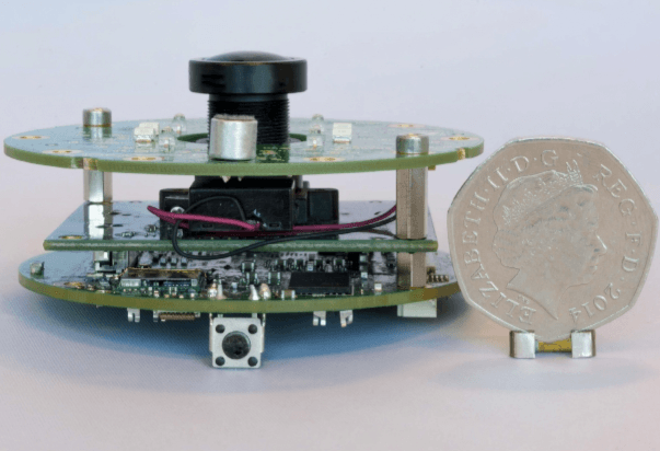
⏩ TL;DR: Why ATEX certification fails - common IS design gotchas
Most ATEX and IECEx submissions fail for the same handful of reasons, and nearly all of them trace back to decisions made weeks or months before the design ever reached a notified body.
- Component energy limits set incorrectly at schematic stage.
- Insufficient PCB creepage and clearance.
- An incomplete dual-fault assessment.
- Gaps in the technical file.
- A test plan agreed too late, or not agreed at all.
Each one is preventable if it's caught during design rather than during certification. A short feasibility study at the start of a project, run alongside your notified body, catches most of them before a single track is routed.
Table of Contents
What happens when an ATEX submission fails?
A project comes in on time and on budget. The design works, the prototype performs, and all that’s left is confirmation that it meets ATEX intrinsic safety requirements.
Then the notified body’s report comes back, and it’s a fail.
At that point, a project where everything went right looks like the opposite. The design has to go back to schematic or layout, sometimes both, and the retest queue at the notified body adds further delay on top of the rework itself. Senior leadership needs telling that the timeline has moved. So do customers who were expecting a certified product on a fixed date.
None of this is unusual.
Certification failure is one of the most common reasons ATEX and IECEx projects slip, and it’s almost always avoidable.
The causes are well understood, and they cluster around five points in the design process.
1. Incorrect component energy limits
This is generally the most common failure point, and it starts at the schematic stage, long before layout begins.
There’s no single “safe” energy figure that applies to an entire gas group. IEC 60079-11 uses ignition curves that depend on your circuit’s voltage, current, source characteristic, protection level and applicable safety factors, not one fixed ceiling.
Gas Group IIC covers highly ignition-sensitive gases including hydrogen and acetylene. Hydrogen’s minimum ignition energy is commonly quoted at around 19µJ, but that figure applies to hydrogen specifically, under specific test conditions.
It isn’t a limit you can apply directly to your own circuit without working through the standard’s tables and curves for your actual design.
Designs fail when engineers estimate energy limits from memory, or reuse a figure from a previous project without re-checking it against the current circuit’s voltage and protection level.
What to do instead
- Check every rail against IEC 60079-11's relevant ignition curves before layout starts. It's worth a few hours of calculation against the standard, to avoid a guess carried over from the last project.
 What to do instead
2. Insufficient PCB creepage and clearance
The next most common failure point shows up once the board is laid out.
IEC 60079-11 specifies minimum creepage and clearance distances based on voltage and pollution degree, and they’re tighter than most engineers expect coming from general commercial PCB design.
This affects the physical separation between intrinsically safe and non-intrinsically safe sections of the board, and it affects component placement, since high-voltage parts can compromise an IS circuit through surface tracking even when the schematic is correct.
A board that passes every electrical check on paper can still fail on a 2mm gap that should have been wider.
- Run design rule checks against IEC 60079-11 spacing requirements before the board goes to fabrication. Catching a 2mm gap on screen costs nothing. Catching it after manufacture costs a respin.
3. Incomplete dual-fault assessment
Zone 0 designs (Ex ia) have to remain intrinsically safe even when two protective components fail simultaneously, not just one.
This is the dual-fault requirement, and it’s where a lot of otherwise solid designs come unstuck.
The notified body will test your circuit against the worst-case combination of failures your protection components could plausibly experience: a Zener diode failing short, a current-limiting resistor failing open, both at once.
If your design has only been checked against single-fault conditions, or against the faults you assumed were most likely rather than the full set the standard requires, it will come back rejected.
- Model every countable fault pair in your protection architecture before you submit. If two Zener diodes can fail together, prove the third still holds.
4. Gaps in the technical file
Not every failure is electrical. A design can be sound and still fail because the documentation supporting it isn’t complete enough for the notified body to assess.
This usually shows up as gaps in the risk assessment, or a bill of materials that doesn’t give full traceability back to certified, dual-approved components.
Notified bodies can’t sign off on a design they can’t fully audit on paper, however well it performs on the bench.
- Build the technical file as you design, not after. Log traceability and risk assessment alongside the schematic, so there's nothing to reconstruct once the hardware is finished.
5. Thin or late test plan
The last common failure point is procedural rather than technical.
If there’s no agreed method for demonstrating compliance under test, or the test plan is only put together once the design is already submitted, the notified body has nothing to assess the design against.
- Agree the test plan with the notified body at the same time as the architecture review. You'll know exactly what you're being tested against before you've committed to a layout.
Five checks, done at the right time. None of them require reinventing how you work, just moving each one earlier in the process.
Why do these ATEX certification mistakes happen- even on well-run projects?
None of the five failure points above are obscure. Most experienced hardware teams already understand power budgets, creepage and clearance, and fault tolerance in general terms. So, generally, lack of knowledge isn’t the issue.
What catches teams out is a handful of edges specific to ATEX work that don’t come up in general commercial PCB design.
Component size is one of them. The maximum temperature a part can reach under fault conditions is tied to its surface area, so the general drift towards smaller packages runs directly against intrinsically safe design.
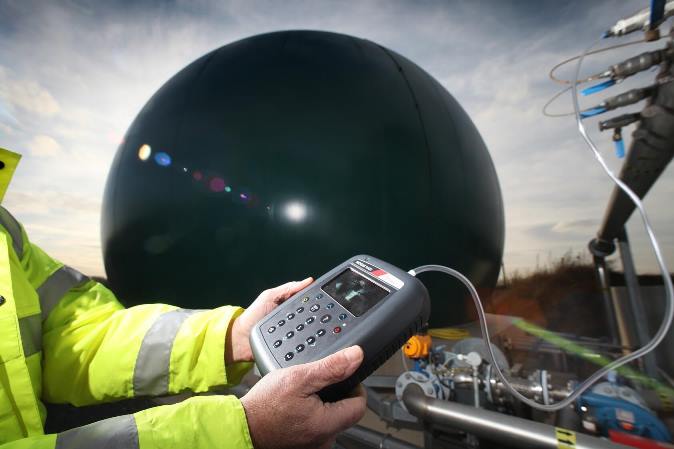
A larger package is often the simpler fix, and it usually costs less engineering time than the thermal analysis needed to justify a smaller one. We ran into this trade-off directly on the Geotech gas analyser, a full custom board built for Zone 0 certification.
Radio modules cause a different problem. Most IoT devices need one, and you have no visibility into what’s inside a third-party module, or control over it. It also sits under separate directives, including the Radio Equipment Directive, which layers EMC and cybersecurity requirements on top of ATEX.
We’ve run into this directly on radio-enabled Zone 0 hardware, including the WAND Remote Data Collector, an 8-channel ultrasonic sensor with Bluetooth 5.0 built in.
Where a component can’t be assessed against standard intrinsic safety techniques, encapsulation under IEC 60079-18 is the usual route: the circuit is cast in resin, and temperature calculations are made on the resin as a whole rather than the components inside it.
It costs more and brings its own rules, but it’s a legitimate way to certify a design that intrinsic safety alone can’t cover.
Then there’s the US market. HazLoc uses broadly the same underlying calculations as ATEX, though the documentation differs. If a product needs both, decide that at the start. Bolting HazLoc on after ATEX certification is already underway costs more time than designing for both from day one.
How a feasibility study catches ATEX certification problems early
Every failure point above is cheaper to catch before layout than after certification. A feasibility study at the start of a project, typically lasting one to two weeks, is where this happens.
The study isn’t a sanity check so much as where the real architectural decisions get made: how much redundancy the protection circuits need, whether encapsulation is required anywhere, and what the power budget actually allows against the product’s functional requirements.
Getting the notified body involved at the end of it, to review those choices before detailed design begins, is what turns “submit and hope” into a design built to pass first time.
Set expectations on timescale from the outset. A reasonable rule of thumb is to plan for roughly double the development time of an equivalent non-ATEX project.
The calculations, the checking, and the back-and-forth with the notified body all add time, and test houses are frequently busy. Build that into the project plan from day one rather than discovering it halfway through.
Not every ATEX product needs this level of scrutiny. A simple pilot light on a DIN rail, or a low-complexity sensor, doesn’t carry the same risk as a multi-channel IoT device with wireless connectivity and onboard signal processing. The feasibility study is where that distinction gets made too.
Get your ATEX design reviewed before the notified body does
ATEX Certification Failures FAQs
Can an ATEX design be fixed after it fails certification, or does it need a full redesign?
It depends on where the failure occurred. A creepage and clearance issue caught at PCB stage may only need a layout revision. A fundamental energy budget or architecture problem, discovered late, often means going back to schematic, which is the kind of work our Design Rescue Service handles. This is why catching issues during a feasibility study, rather than at the notified body, matters so much for cost and timeline.
How long does ATEX certification take if the design is right the first time?
Well-designed products with complete documentation generally move through certification faster than those with outstanding issues, since there’s no rework-and-retest cycle to work through. The exact timeline depends on the complexity of the design and the notified body’s current workload.
What's the difference between a countable fault and a non-countable fault?
A countable fault is a specific, foreseeable failure mode in a protection component, such as a Zener diode failing short. Zone 0 (Ex ia) designs must remain safe even when two countable faults occur simultaneously. Non-countable faults, such as PCB track clearance issues, are assumed to be present under worst-case conditions and are assessed separately.
Do I need a feasibility study for a simple ATEX product like a pilot light?
Not necessarily. Low-complexity products with a small, well-understood set of components carry less architectural risk than complex, multi-function devices. The feasibility study is most valuable where the architecture itself involves real decisions, such as redundancy levels, encapsulation, or a tight power budget against demanding functionality.
Is HazLoc certification the same as ATEX?
No, but the two aren’t unrelated. HazLoc in the US is built on broadly similar technical calculations to ATEX, though the documentation requirements differ. A product intended for both markets should be designed with both in mind from the start.

Dunstan is a chartered electronics engineer who has been providing embedded systems design, production and consultancy to businesses around the world for over 30 years.
Dunstan graduated from Cambridge University with a degree in electronics engineering in 1992. After working in the industry for several years, he co-founded multi-award-winning electronics engineering consultancy ByteSnap Design in 2008. He then went on to launch international EV charging design consultancy Versinetic during the 2020 global lockdown.
An experienced conference speaker domestically and internationally, Dunstan covers several areas of electronics product development, including IoT, integrated software design and complex project management.
In his spare time, Dunstan enjoys hiking and astronomy.
Expand your knowledge
- ATEX and Intrinsic Safety: Design for Harsh Environments
- How to Manage an Intrinsically Safe Power Budget for Zone 0
- ATEX vs IECEx: 2026 Guide to Hazardous Area Certification
- ATEX Product Design Services
- IEC 60079-11: Intrinsic Safety “i” Protection
- HSE Guidance on DSEAR (Dangerous Substances and Explosive Atmospheres Regulations)
- UK ATEX Equipment Directive (Statutory Instruments)
- EU ATEX Directive 2014/34/EU
- IECEx System Homepage